

Solutions & Capabilities
CloudGate’s solutions focus on compound semiconductor materials and wafer manufacturing, with an emphasis on MOCVD epitaxial growth and InP substrate-related production. From process planning and engineering development to controlled manufacturing execution, we establish robust, scalable processes aligned with customer specifications and application needs.
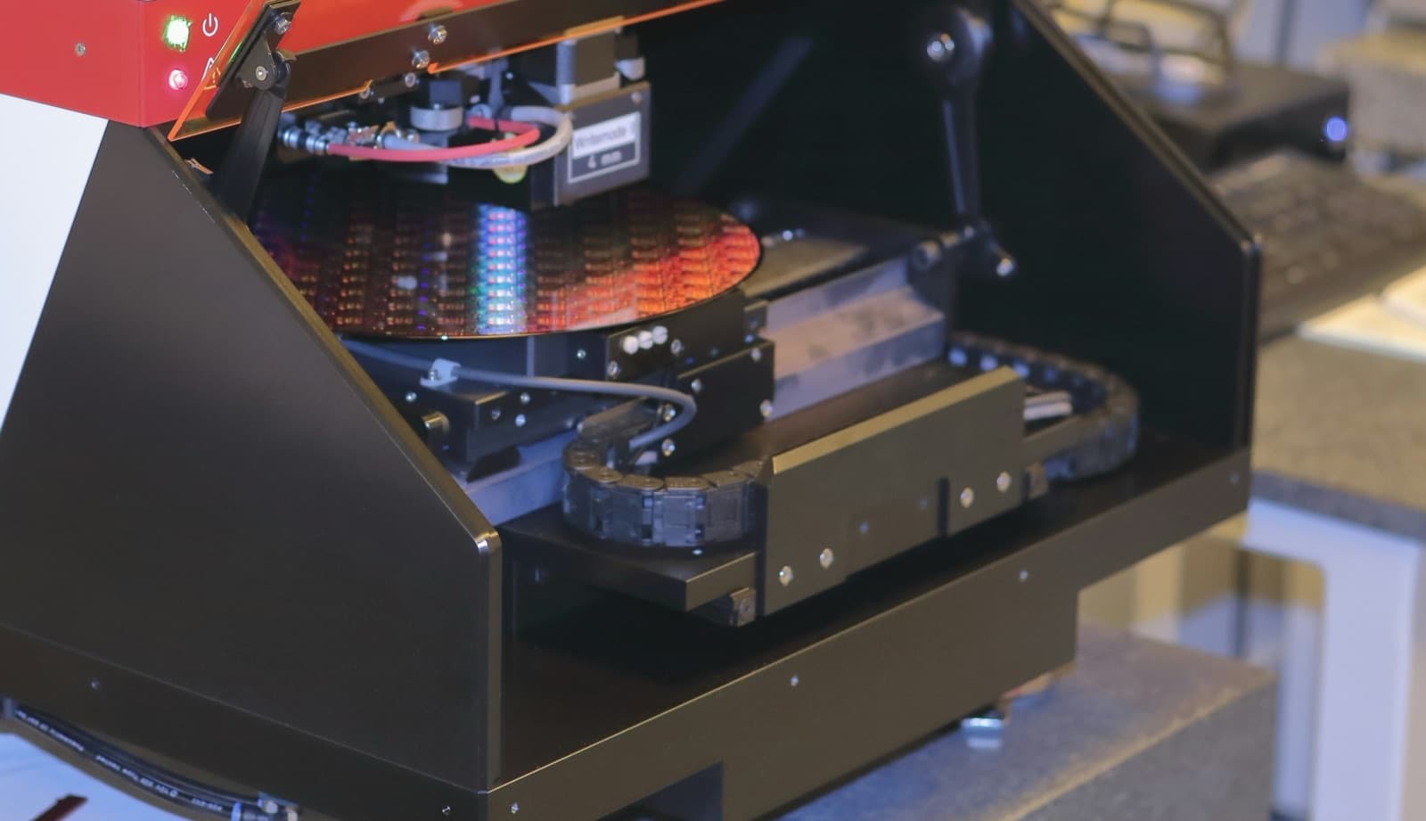
MOCVD Epitaxial Growth & Process Development
CloudGate offers comprehensive Metal-Organic Chemical Vapor Deposition (MOCVD) process development services for compound semiconductor structures. We specialize in precision gas-phase epitaxy to produce uniform, high-crystallinity thin-film layers tailored to photonic and optoelectronic devices. Through rigorous control over chamber thermodynamics, gas flow dynamics, and deposition rates, we ensure high run-to-run repeatability and defect minimization.
- Advanced MOCVD reactor parameter optimization for compound semiconductor structures
- Atomic-scale layer thickness uniformity and precise composition control
- High run-to-run repeatability with documented recipe management
- Custom epitaxial layer growth tailored for lasers, modulators, and photodetectors
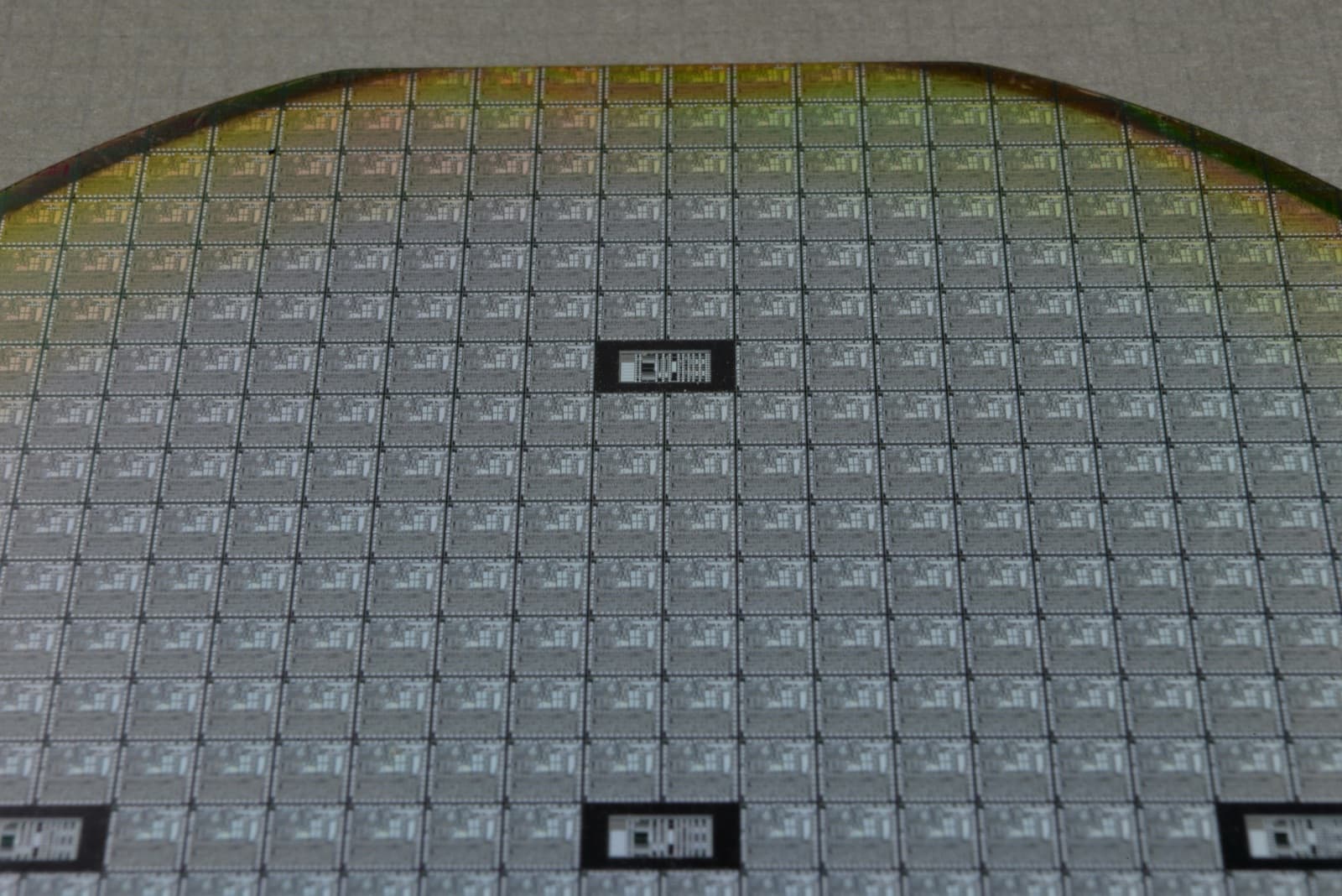
InP Substrate & Optoelectronic Wafer Solutions
We deliver tailored Indium Phosphide (InP) substrate handling, preparation, and epitaxial wafer production pathways. InP is the material of choice for high-speed optical transceivers, telecom lasers, and photonic integrated circuits (PICs) due to its superior electron velocity and direct bandgap properties. CloudGate provides customer-aligned wafer solutions with stringent surface quality, ultra-low defect densities, and comprehensive post-epi characterization.
- Optimized production workflows for Indium Phosphide (InP) based wafers
- High-performance substrate preparation supporting high-speed telecom & datacom optics
- Strict surface defect inspection, roughness control, and wafer bow/warp verification
- Compatibility with downstream semiconductor fabrication and diced die assembly
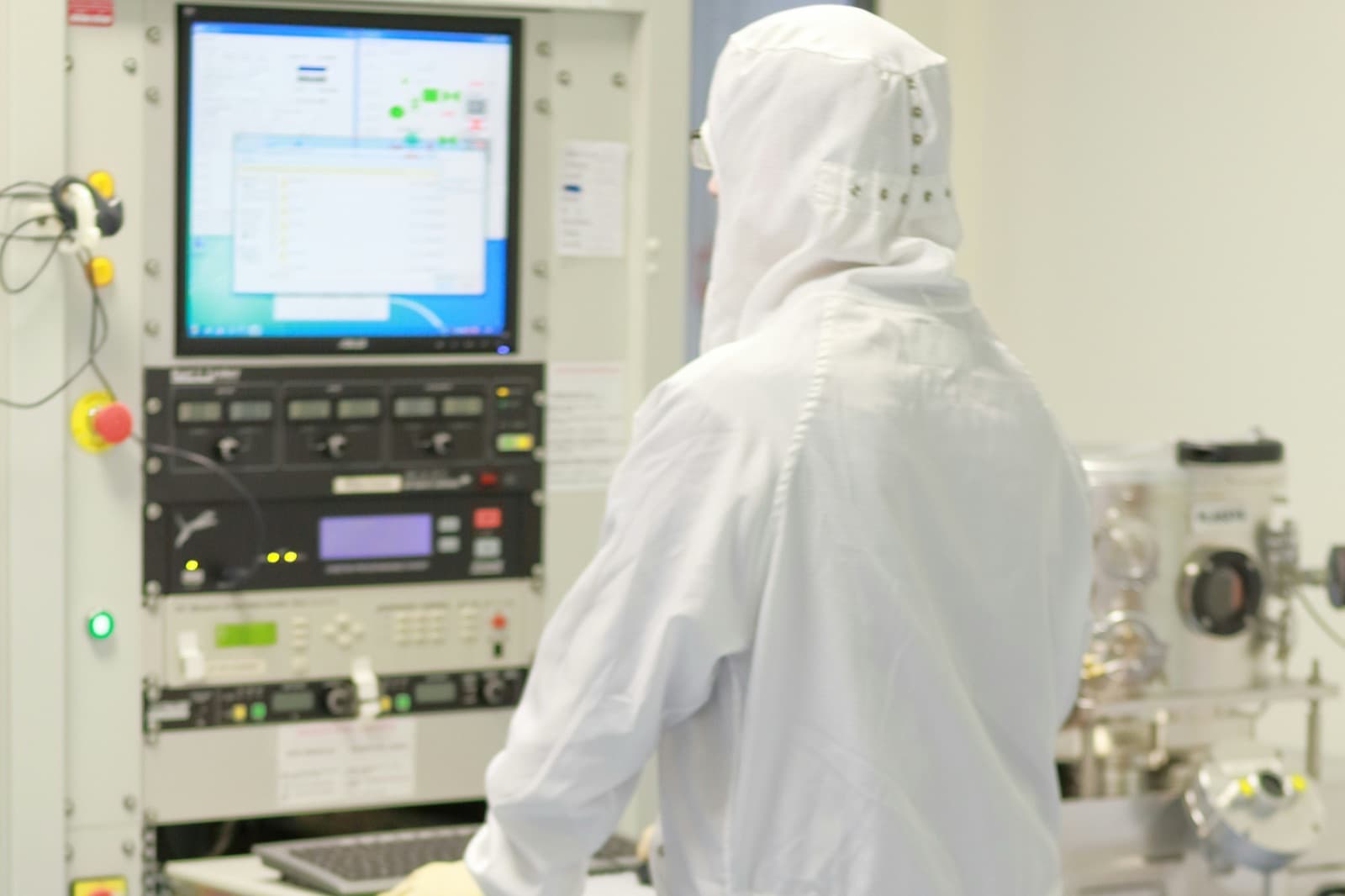
Process Engineering & Scalable Production Planning
Bridging laboratory-level recipe formulation to high-yield commercial production requires disciplined engineering governance. CloudGate utilizes structured production planning, design-of-experiments (DOE), and statistical process control (SPC) to optimize process windows. Our cross-functional engineering teams align tool maintenance, recipe calibration, and workflow logistics to build a seamless path from pilot batches to mass production.
- Design of Experiments (DOE) and process window optimization for rapid recipe maturation
- Statistical Process Control (SPC) integration to minimize process drift and maximize yield
- Cross-functional engineering coordination between R&D, operations, and quality teams
- Scalable manufacturing architecture ready for commercial-volume expansion
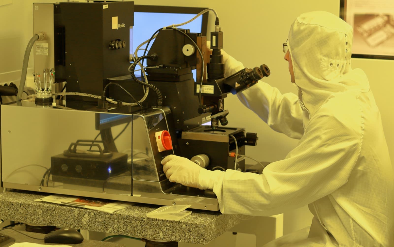
Quality Assurance, In-Process Control & Full Traceability
Every production run at CloudGate is governed by strict standard operating procedures (SOPs) and comprehensive in-line verification. We maintain end-to-end material and batch traceability from raw precursor gases and substrates to finished wafers. By embedding real-time monitoring and systematic root-cause analysis, we guarantee consistent quality, audit readiness, and elevated customer confidence.
- 100% batch-level and wafer-level traceability across all production stages
- Real-time in-process parameter monitoring and automated alert protocols
- Documented Quality Management System aligned with ISO 9001 standards
- Systematic non-conformance management and continuous improvement (Kaizen) cycles
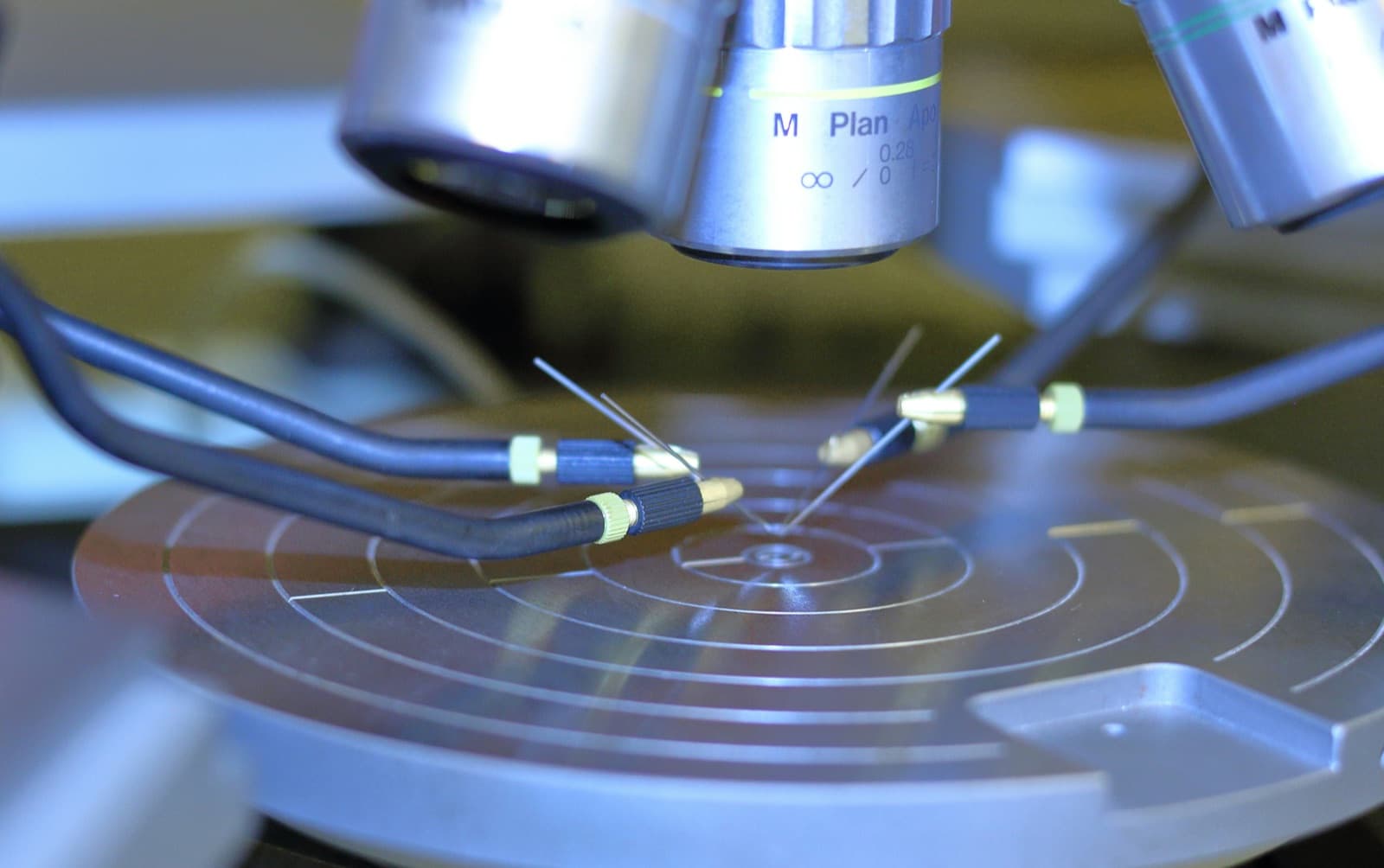
Advanced Analytical Characterization & Reliability Testing
Leveraging advanced analytical capabilities within our manufacturing ecosystem, CloudGate provides comprehensive structural, optical, and electrical characterization for compound semiconductor layers. Through methods such as high-resolution X-ray diffraction (HRXRD), photoluminescence (PL) mapping, and surface profiling, we validate material integrity before downstream customer integration.
- High-Resolution X-Ray Diffraction (HRXRD) for crystal quality and layer thickness verification
- Photoluminescence (PL) mapping for optical wavelength uniformity evaluation
- Non-destructive wafer surface inspection and particle count verification
- Reliability stress testing data supporting customer device qualifications